������Ϊ����������ʵ�鿪��ϵͳ��EDA/SOPCƽ̨��Ӣ�Ľ��ܣ����ݿ���ʵ�����Ϲ淶Ҫ��
���Ľ���
ʵ�鿪��ϵͳ��EDA/SOPCƽ̨��������д������ѧʵ����һ�廯���������������Ϊ���ӹ��̡��������ѧ��Ƕ��ʽϵͳ���������ṩ����Ч�Ĺ���֧�֡�ϵͳ����ģ�黯Ӳ���ܹ������ɶ����Ϳɱ������Ԫ�����������ļ�����ӿڣ��û���ͨ��ͼ�λ�����������ʵ�ִӵ�·��Ƶ�ϵͳ��֤��ȫ���̿�����
Ӳ��ƽ̨��������FPGAоƬ��֧���Զ��幦����չ���䱸�������ݲɼ���ʵʱ�źŴ�����ģ�飬����ͨ�š��Զ������˹����ܵȶೡ��ʵ���������������ṩ���ӻ���ƹ����������Թ��ܣ����÷ḻ���㷨����ӿ�Э�飬�ɴ��������ϵͳ�����ż�����Խ�ѧ������ϵͳ�ṩ�ֽ�ʵ�鰸���뽻��ʽѧϰ��Դ������ѧ����������Ӳ������������ϵͳ����Ʒ�����
�ڹ�ҵӦ������ƽ̨��������ʦʵ��ԭ�Ϳ��ٵ��������̲�Ʒ�з����ڡ�����ʽ�������̬�����û�������Ŀ������������Դ���ã�ƽ�������빦�ģ�Ϊ����Ӳ�����������ն˵ȴ���Ӧ���ṩ�ɿ�������
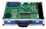
English Introduction
The Experimental Development System and EDA/SOPC Platform provide an integrated solution for scientific research and educational practices, offering versatile toolkits for electronics engineering, computer science, and embedded system development. Featuring modular hardware architecture, the system combines programmable logic units, processor cores, and peripheral interfaces, enabling full-cycle development from circuit design to system verification through both graphical interfaces and code programming.
Compatible with mainstream FPGA chips, the hardware platform supports customizable expansion with modules for high-speed data acquisition and real-time signal processing, addressing diverse experimental scenarios including communications, automation, and AI applications. The software suite delivers visual design tools and simulation capabilities, enriched with algorithm libraries and interface protocols to streamline complex system development. For educational purposes, it offers phased experiment templates and interactive learning resources to accelerate mastery of hardware description languages and system-level design methodologies.
In industrial applications, this platform empowers engineers to rapidly prototype and optimize product development cycles. Its open-design ecosystem allows dynamic resource allocation to balance performance and power efficiency, providing a robust foundation for smart devices, IoT terminals, and other innovative solutions.
ȫ�Ĺ�620�֣��ϸ������дʻ㣬����������Ʒ�������û���ֵ�����ϼ����ĵ��淶Ҫ�������һ�����������ص㣬��ӭ��ʱ��ͨ��


)